AMD Unveils Their Embedded+ Architecture, Ryzen Embedded with Versal Together
by Gavin Bonshor on February 6, 2024 9:00 AM EST- Posted in
- CPUs
- AMD
- Embedded
- SoCs
- Ryzen
- Ryzen Embedded
- Versal
- Ryzen Embedded R2314
One area of AMD's product portfolio that doesn't get as much attention as the desktop and server parts is their Embedded platform. AMD's Embedded series has been important for on-the-edge devices, including industrial, automotive, healthcare, digital gaming machines, and thin client systems. Today, AMD has unveiled their latest Embedded architecture, Embedded+, which combines their Ryzen Embedded processors based on the Zen+ architecture with their Versal adaptive SoCs onto a single board.
The Embedded+ architecture integrates the capabilities of their Ryzen Embedded processors with their Versal AI Edge adaptive SoCs onto one packaged board. AMD targets key areas that require good computational power and power efficiency. This synergy enables Embedded+ to handle AI inferencing and manage complex sensor data in real-time, which is crucial for applications in dynamic and demanding environments.
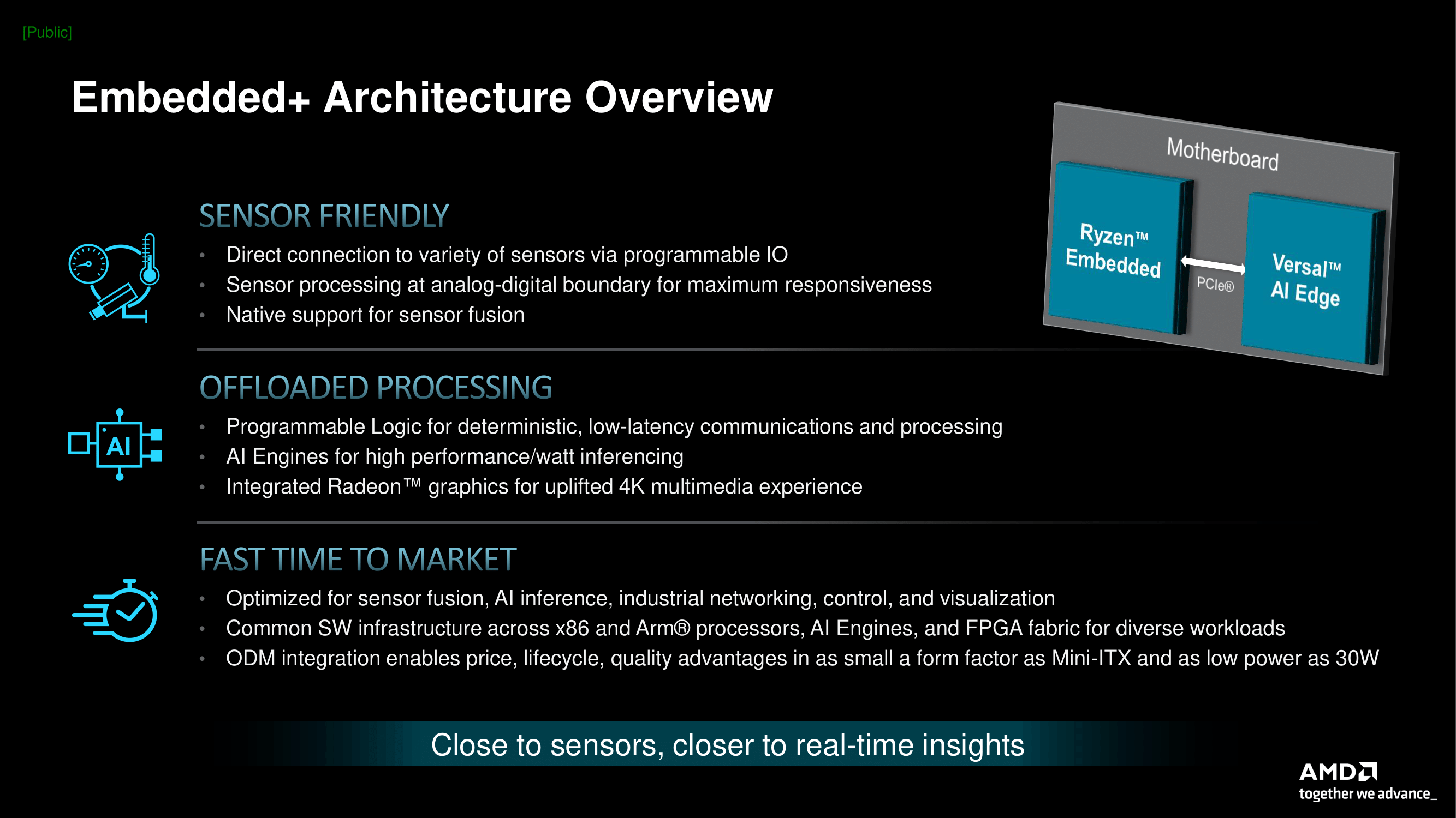
Giving ODMs the ability to have both Ryzen Embedded and their Versal SoCs onto a single board is particularly beneficial for industries requiring low-latency response times between hardware and software, including autonomous vehicles, diagnostic equipment in healthcare, and precision machinery in industrial automation. The AMD Embedded+ architecture can also support various workloads across different processor types, including x86 and ARM, along with AI engines and FPGA fabric, which offers flexibility and scalability of embedded computing solutions within industries.
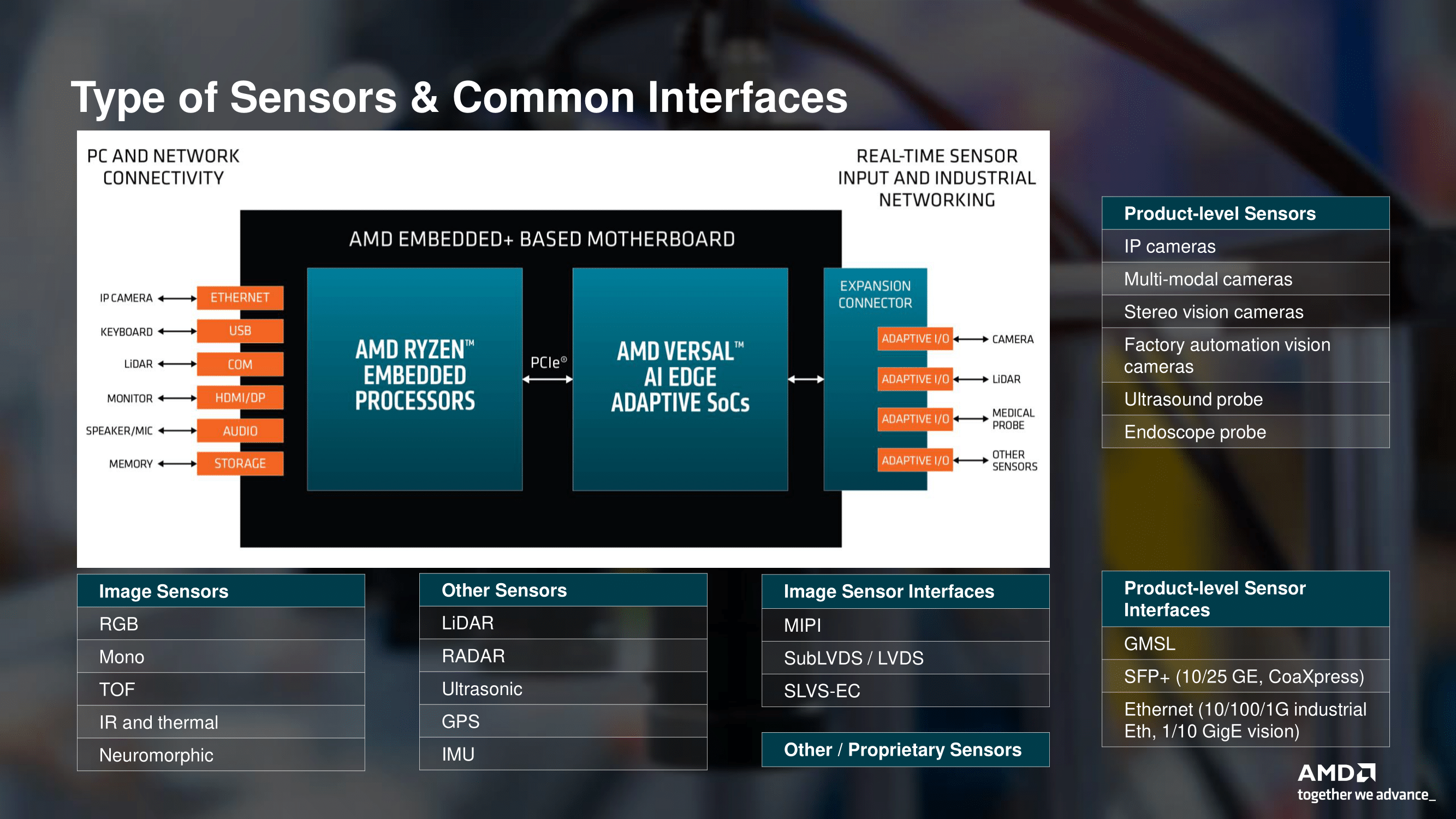
The Embedded+ platform from AMD offers plenty of compatibility with various sensor types and their corresponding interfaces. It facilitates direct connectivity with standard peripherals and industrial sensors through Ethernet, USB, and HDMI/DP interfaces. The AMD Ryzen Embedded processors within the architecture can handle inputs from traditional image sensors such as RGB, monochrome, and even advanced neuromorphic types while supporting industry-standard image sensor interfaces like MIPI and LVDS.
Further enhancing its capability, the AMD Versal AI Edge adaptive SoCs on the Embedded+ motherboard offer adaptable I/O options for real-time sensor input and industrial networking. This includes interfacing with LiDAR, RADAR, and other delicate and sophisticated sensors necessary for modern embedded systems in the industrial, medical, and automotive sectors. The platform's support for various product-level sensor interfaces, such as GMSL and Ethernet-based vision protocols, means it is designed and ready for integration into complex, sensor-driven systems.
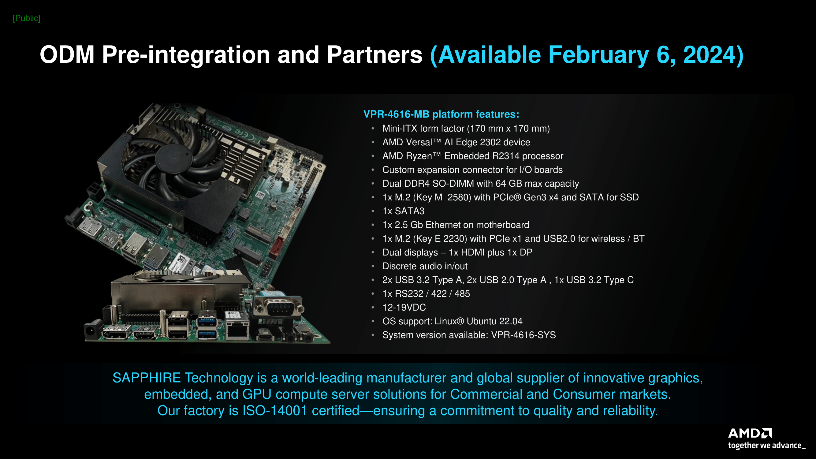
AMD has also announced a new pre-integrated solution, which will be available for ODMs starting today. The Sapphire Technology VPR-4616-MB platform is a compact, Mini-ITX form factor motherboard that leverages the AMD Versal AI Edge 2302 SoC combined with an AMD Ryzen Embedded R2314 processor, which is based on Zen+ and has 4C/4T with 6 Radeon Vega compute units. It features a custom expansion connector for I/O boards, supporting a wide array of connectivity options, including dual DDR4 SO-DIMM slots with up to 64 GB capacity, one PCIe 3.0 x4 M.2 slot, and one SATA port for conventional HDDs and SSDs, The VPR-4616-MB also has a good array of networking capabilities including 2.5 Gb Ethernet and an M.2 Key E 2230 PCIe x1 slot for a wireless interface. It also supports the Linux-based Ubuntu 22.04 operating system.
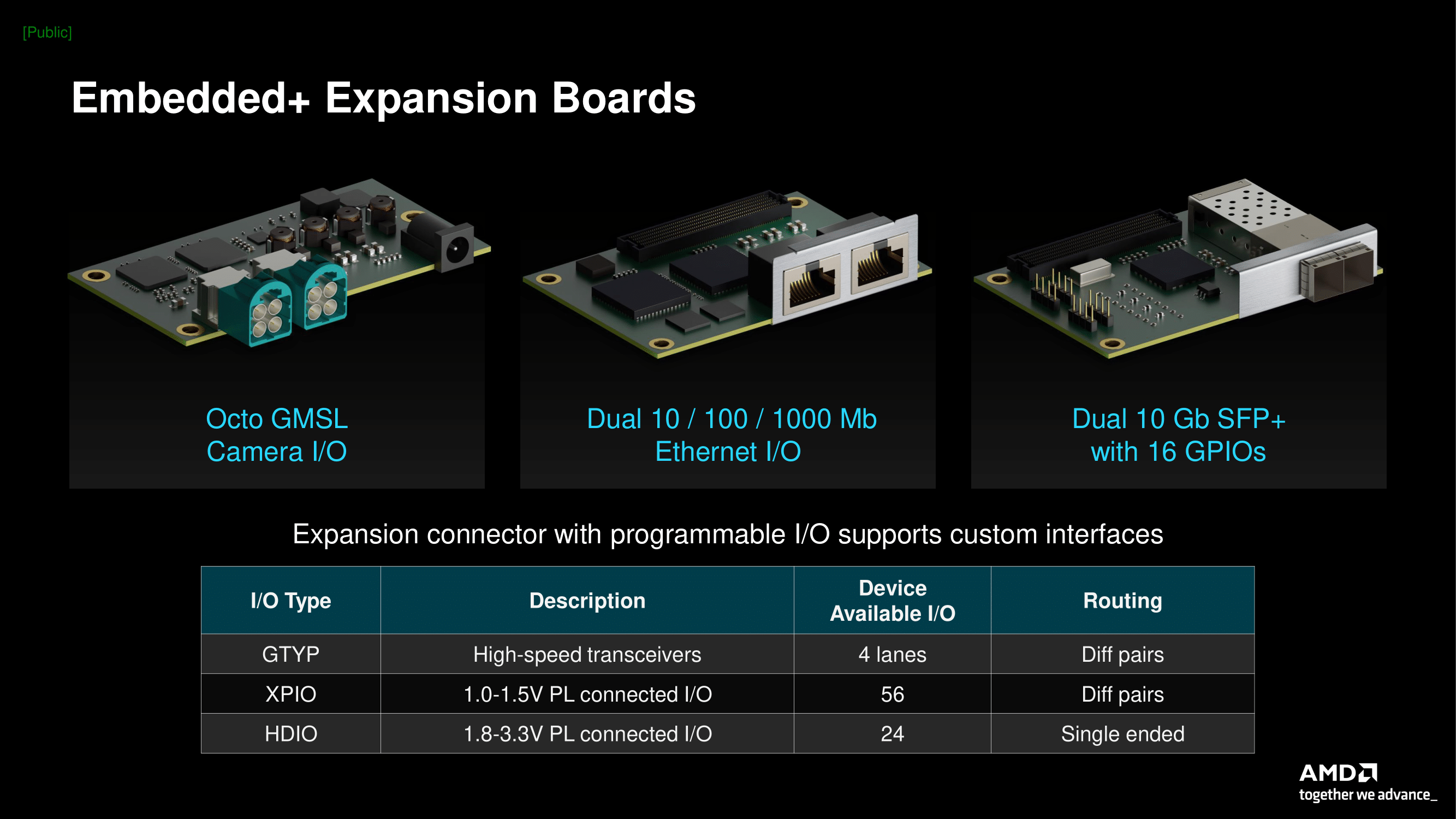
Also announced is a series of expansion boards that significantly broaden support for the Embedded+ architecture. The Octo GMSL Camera I/O board is particularly noteworthy for its ability to interface with multiple cameras simultaneously. It is undoubtedly suitable for high bandwidth vision-based systems, integral to sectors such as advanced driver-assistance systems (ADAS) and automated surveillance systems. These systems often require the integration of numerous image inputs for real-time processing and analysis, and the Octo GMSL board is engineered to meet this demand specifically.
Additionally, a dual Ethernet I/O board is available, capable of supporting 10/100/1000 Mb connections, catering to environments that demand high-speed network communications. The Dual 10 Gb SFP+ board has 16 GPIOs for even higher bandwidth requirements, providing ample data transfer rates for tasks like real-time video streaming and large-scale sensor data aggregation. These expansion options broaden the scope of what the Embedded+ architecture is capable of in an edge and industrial scenario.
The Sapphire VPR-4616-MB is available for customers to purchase now and in a complete system configuration, including storage, memory, power supply, and chassis.
_thumb.png)
_thumb.png)
_thumb.png)
_thumb.png)
_thumb.png)
_thumb.png)


11 Comments
View All Comments
mukiex - Tuesday, February 6, 2024 - link
A silent prayer for a cheap FPGA dev board that's a step above the De-10 Nano.Threska - Tuesday, February 6, 2024 - link
Looks interesting. No prices, and the software is going to be what makes or breaks this.trisct - Tuesday, February 6, 2024 - link
Absolutely agree Threska. A new processing board isn't going to impress anyone unless there is a degree of integration available with software libraries (a la CUDA). Nvidia pairs their hardware with a capable and well tested software layer. There's the way to make real money.erinadreno - Tuesday, February 6, 2024 - link
That CPU is not sufficient for developing on the very FPGA on the same PCB. Nor is there enough board space for all the high speed io. Seems like the worse of both worlds.drajitshnew - Tuesday, February 6, 2024 - link
The 3rd slide says "2580 M-key" slot. Is that an error or there is a new standard?Xajel - Wednesday, February 7, 2024 - link
It's a new standard, not very new but it was promoted with the PCIe 5.0 devices coming, first mentioned 2 years ago with some leaked info about Gigabyte X670E motherboards supporting 25110 M.2. And they do support these (Like the X670 Aorus Elite AX).meacupla - Wednesday, February 7, 2024 - link
to add, 2280 will fit in a 2580 slot. The pin-out is the same, it's just 1.5mm wider on each side.Samus - Wednesday, February 7, 2024 - link
2580 is basically the width of many LTE\5G modems that traditionally go in 2242 sockets and overlap. I suspect they are trying to make headroom for larger SSD's or more complex PCIe M2 devices...or maybe just headroom for a heatsink\heat dissipation. I saw a few SBC's at CES with 2580 sockets but they just had 2280 cards installed.kn00tcn - Thursday, February 8, 2024 - link
zen+? GF contract strikes again?Bruzzone - Friday, February 9, 2024 - link
Kicked Arm out as the processor of choice in Xilinx FPGA's? mb