The Tegra 4 GPU, NVIDIA Claims Better Performance Than iPad 4
by Anand Lal Shimpi on January 14, 2013 6:13 PM ESTAt CES last week, NVIDIA announced its Tegra 4 SoC featuring four ARM Cortex A15s running at up to 1.9GHz and a fifth Cortex A15 running at between 700 - 800MHz for lighter workloads. Although much of CEO Jen-Hsun Huang's presentation focused on the improvements in CPU and camera performance, GPU performance should see a significant boost over Tegra 3.
The big disappointment for many was that NVIDIA maintained the non-unified architecture of Tegra 3, and won't fully support OpenGL ES 3.0 with the T4's GPU. NVIDIA claims the architecture is better suited for the type of content that will be available on devices during the Tegra 4's reign.
Despite the similarities to Tegra 3, components of the Tegra 4 GPU have been improved. While we're still a bit away from a good GPU deep-dive on the architecture, we do have more details than were originally announced at the press event.
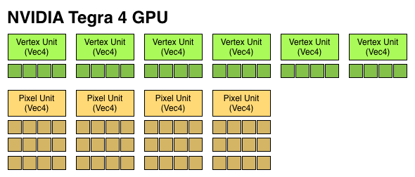
Tegra 4 features 72 GPU "cores", which are really individual components of Vec4 ALUs that can work on both scalar and vector operations. Tegra 2 featured a single Vec4 vertex shader unit (4 cores), and a single Vec4 pixel shader unit (4 cores). Tegra 3 doubled up on the pixel shader units (4 + 8 cores). Tegra 4 features six Vec4 vertex units (FP32, 24 cores) and four 3-deep Vec4 pixel units (FP20, 48 cores). The result is 6x the number of ALUs as Tegra 3, all running at a max clock speed that's higher than the 520MHz NVIDIA ran the T3 GPU at. NVIDIA did hint that the pixel shader design was somehow more efficient than what was used in Tegra 3.
If we assume a 520MHz max frequency (where Tegra 3 topped out), a fully featured Tegra 4 GPU can offer more theoretical compute than the PowerVR SGX 554MP4 in Apple's A6X. The advantage comes as a result of a higher clock speed rather than larger die area. This won't necessarily translate into better performance, particularly given Tegra 4's non-unified architecture. NVIDIA claims that at final clocks, it will be faster than the A6X both in 3D games and in GLBenchmark. The leaked GLBenchmark results are apparently from a much older silicon revision running no where near final GPU clocks.
| Mobile SoC GPU Comparison | |||||||||||||||
| GeForce ULP (2012) | PowerVR SGX 543MP2 | PowerVR SGX 543MP4 | PowerVR SGX 544MP3 | PowerVR SGX 554MP4 | GeForce ULP (2013) | ||||||||||
| Used In | Tegra 3 | A5 | A5X | Exynos 5 Octa | A6X | Tegra 4 | |||||||||
| SIMD Name | core | USSE2 | USSE2 | USSE2 | USSE2 | core | |||||||||
| # of SIMDs | 3 | 8 | 16 | 12 | 32 | 18 | |||||||||
| MADs per SIMD | 4 | 4 | 4 | 4 | 4 | 4 | |||||||||
| Total MADs | 12 | 32 | 64 | 48 | 128 | 72 | |||||||||
| GFLOPS @ Shipping Frequency | 12.4 GFLOPS | 16.0 GFLOPS | 32.0 GFLOPS | 51.1 GFLOPS | 71.6 GFLOPS | 74.8 GFLOPS | |||||||||
Tegra 4 does offer some additional enhancements over Tegra 3 in the GPU department. Real multisampling AA is finally supported as well as frame buffer compression (color and z). There's now support for 24-bit z and stencil (up from 16 bits per pixel). Max texture resolution is now 4K x 4K, up from 2K x 2K in Tegra 3. Percentage-closer filtering is supported for shadows. Finally, FP16 filter and blend is supported in hardware. ASTC isn't supported.
If you're missing details on Tegra 4's CPU, be sure to check out our initial coverage.


59 Comments
View All Comments
Scannall - Monday, January 14, 2013 - link
Considering their past performance I'll wait for the independent benchmarks. Regardless though, the SOC wars are looking interesting. Though the PowerVR 6 series (Rogue) should be shipping this quarter, and is rumored to put out around 210 Gflops. We'll have to wait and see on that one as well.Kevin G - Monday, January 14, 2013 - link
210 GFLOPs for Rogue? That's Xbox 360 class performance which is 240 GLFOPs for comparison.Zink - Monday, January 14, 2013 - link
Xbox games often run in 720p, which just goes to show how much faster these SOCs will need to get to drive over four time that resolution with modern graphics engines.JarredWalton - Monday, January 14, 2013 - link
GFLOPS is not the greatest way of measuring performance, but something interesting to keep in mind is that Rogue is still using the same process technology as PowerVR's current stuff but adding more features (DX10 class stuff, essentially). I'm not sure if we noted this elsewhere, but it's possible that Rogue won't be any faster than the current stuff -- it will just support some newer GPU features.As for Xbox 360, considering it's now over seven years old, I suspect much of the next-gen SoC silicon will at least match it in terms of gaming potential. As usual, it's more about the games than the hardware. Just like on Windows, on Android games need to support a wider array of hardware, so some optimization opportunities get lost.
blanarahul - Tuesday, January 15, 2013 - link
Agreed. BTW ARM's new GPUs( T604, T624, T628, T658 T678 ) use Unified Shader design, right?alex3run - Saturday, January 26, 2013 - link
Yes, mali t6xx use Unified shader design.R0H1T - Tuesday, January 15, 2013 - link
I wonder what it does to the power efficiency though considering the fact that the Apple custom SoC lag on the CPU front, bear in mind that it'll also take more space on the die itself, not to mention they're pretty infamous for over heating, maybe that's just the cheap aluminium !Basically what I'm trying to say here is that on the same process node, that you mentioned above, PowerVR has very little to no room for making this an efficient & better performing GPU than the 5x series(relatively speaking) also most of the performance gains would be had by adding more silicon rather than optimizing the GPU, that'll be done perhaps later on just not right now ?
Kevin G - Tuesday, January 15, 2013 - link
Indeed. ROP count, TMU count and memory bandwidth all contribute to performance. Considering the high resolution displays becoming popular in the mobile space, it'd make sense to scale the number of ROP's and TMU's alongside shader performance. The real telling difference between this and the Xbox 360 in terms of raw hardware is that the Xbox 360 has a 10 MB of eDRAM with an incredible amount of bandwidth to. Hence why the Xbox 360 was often marketed with '4x MSAA for free' to developers (though modern deferred rendering engine can't take advantage of it).ARM SoC's on the other hand have had relatively narrow memory buses running at low clock speeds, much less a sizable eDRAM pool. Only chips like the A5X and A6X have bandwidth figures approaching the Xbox 360's main memory bus (17 GB/s vs. 22.6 GB/s). PowerVR does have nice trick up its sleeve using tile based rendering. That conserves a good chunk of memory bandwidth for better efficiency but I doubt it'd be enough offset the benefits eDRAM brings to the XBox 360.
MrSpadge - Tuesday, January 15, 2013 - link
You wouldn't need to run at native res for games on these ultra high density displays. Calculating once for every 4 pixel group would suffice. Only use full resolution for GUI elemtens.piroroadkill - Tuesday, January 15, 2013 - link
Yeah, exactly.It'd be nice to have a 720p/1080p toggle to see if people can actually see the difference at normal distances on those screens.