Intel Reveals New Haswell Details at ISSCC 2014
by Anand Lal Shimpi on February 9, 2014 3:00 PM EST- Posted in
- CPUs
- Intel
- Haswell
- ISSCC
- ISSCC 2014
As of late, Intel has been unusually guarded about releasing information about its microprocessor designs. Haswell launched last year with great architecture disclosure, but very limited disclosure about die sizes, transistor counts and almost anything surrounding the interface between Haswell and its optional embedded DRAM (Crystalwell) counterpart. This week at ISSCC, Intel will finally be filling in some of the blanks.
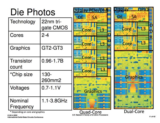
The first bit of new information we have are official transistor counts for the range of Haswell designs. At launch Intel only disclosed transistor counts and die areas for Haswell ULT GT3 (dual-core, on-die PCH, GT3 graphics) and Haswell GT2 (quad-core, no on-die PCH, GT2 graphics). Today we have both the minimum and maximum configurations for Haswell. Note all transistor counts below are schematic not layout:
| Intel Haswell | |||||||||||||||||
| CPU Configuration | GPU Configuration | Die Size | Transistor Count | ||||||||||||||
| 4+3 | Quad-Core | GT3e | 260mm2 + 77mm2 | 1.7B + ? | |||||||||||||
| ULT 2+3 | Dual-Core | GT3 | 181mm2 | 1.3B | |||||||||||||
| ULT 2+2 | Dual-Core | GT2 | ? | (est) ~1B | |||||||||||||
| 4+2 | Quad-Core | GT2 | 177mm2 | 1.4B | |||||||||||||
| 2+2 | Dual-Core | GT2 | 130mm2 | 0.96B | |||||||||||||
I've organized the table above by decreasing die size. I still don't have confirmation for the ULT 2+2 configuration, but the rest is now filled in and accurate. If you remember back to our Iris Pro review, I measured the die area for Haswell GT3 and the Crystalwell eDRAM using some cheap calipers. I came up with 264mm2 + 84mm2, the actual numbers are pretty close at 260mm2 + 77mm2.
Doing some rough math we see that the addition of a third graphics slice to a Haswell core accounts for around 300M transistors. That would put the ULT2+2 configuration at around 1B total transistors. I suspect the ULT 2+2 configuration is similar in size to the quad-core + GT2 configuration.
Next up on the list is some additional information on the Crystalwell (embedded DRAM) design and configuration. Intel explained how it arrived at the 128MB L4 eDRAM cache size, but it wouldn't tell us the operating frequency of the memory or the interface between it and the main CPU die. In its ISSCC disclosures, Intel filled in the blanks:
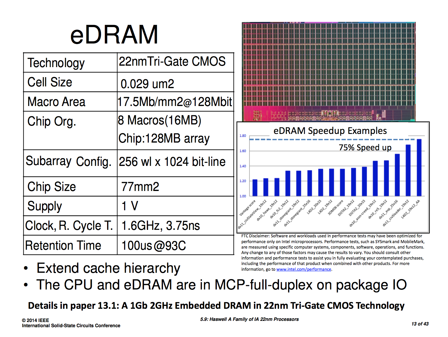
The 128MB eDRAM is divided among eight 16MB macros. The eDRAM operates at 1.6GHz and connects to the outside world via a 4 x 16-bit wide on-package IO (OPIO) interface capable of up to 6.4GT/s. The OPIO is highly scalable and very area/power efficient. The Haswell ULT variants use Intel's on-package IO to connect the CPU/GPU island to an on-package PCH. In this configuration the OPIO delivers 4GB/s of bandwidth at 1pJ/bit. When used as an interface to Crystalwell, the interface delivers up to 102GB/s at 1.22pJ/bit. That amounts to a little under 1.07W of power consumed to transmit/receive data at 102GB/s.
By keeping the eDRAM (or PCH) very close to the CPU island (1.5mm), Intel can make the OPIO extremely simple.
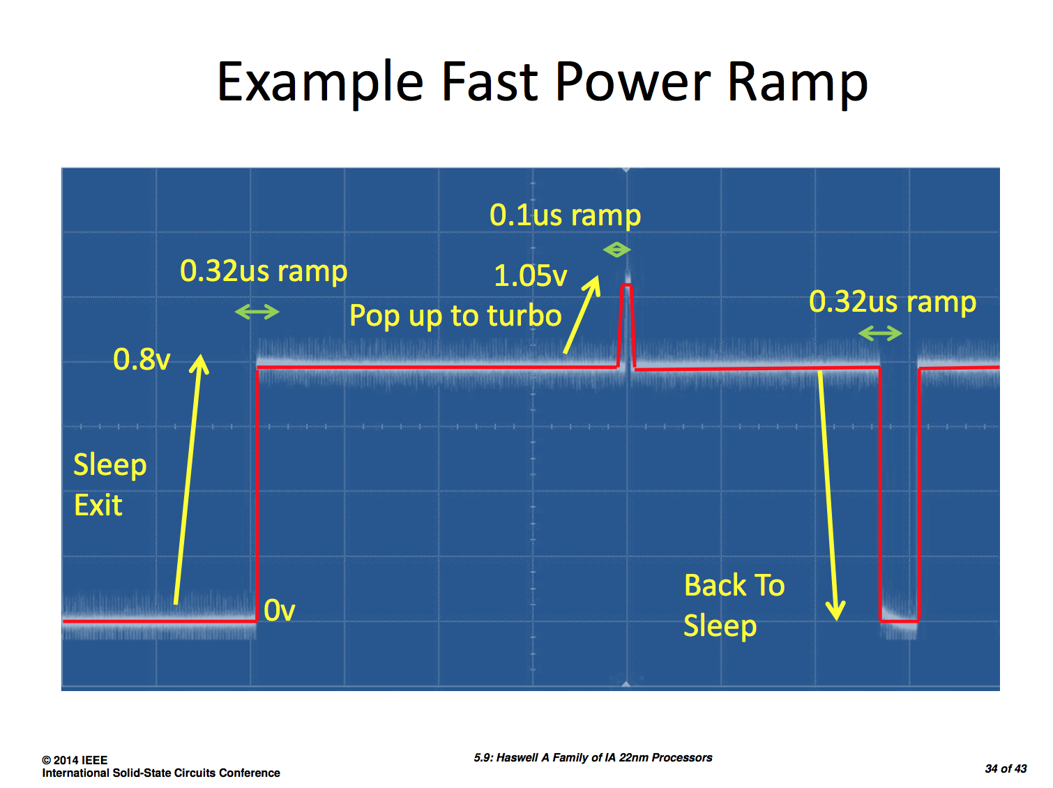
Intel also shared some data on how it achieved substantial power savings with Haswell, including using a new stacked power gate for the memory interface that reduced leakage by 100x over Ivy Bridge. Haswell's FIVR (Full Integrated Voltage Regulator) is also a topic of discussion in Intel's ISSCC papers. FIVR ends up being 90% efficient under load and can enter/exit sleep in 0.32µs, requiring only 0.1µs to ramp up to turbo frequencies.
Intel's Haswell ISSCC disclosures don't really change anything about Haswell, but they do further illustrate just how impressive of a design it is.


44 Comments
View All Comments
Braumin - Sunday, February 9, 2014 - link
It's fascinating to see how they can just keep finding ways to do things better. I'm sure whomever figured out how to reduce leakage on the memory interface by 100x got a nice Christmas bonus!Any word on how Broadwell is coming along? Do you think we'll see it this year or will it be moved to 2015?
przemo_li - Sunday, February 9, 2014 - link
Judging by Linux enablement Broadwell is coming along nicely. 3.14/3.15 should do the job on the kernel side. Mesa is also progressing well. H2 2014 should see Broadwell Out-of-The-Box experience on decent level for stable Linux distros.TheinsanegamerN - Sunday, February 9, 2014 - link
so, it should be out H2 2014 then?Krysto - Monday, February 10, 2014 - link
If they're still announcing "new" Haswell chips at this point, then at best we'll see a couple of Broadwell designs ship by Christmas, but definitely in no "mass market" capacity.toyotabedzrock - Monday, February 10, 2014 - link
Right before the Kernel for Linux reaches 3.15 or right after.All the basics for broadwell have been added for 3.14 but are partly disabled on the gpu side by default. The pci ids where added already.
masimilianzo - Sunday, February 9, 2014 - link
Any word on Broadwell? I heard it will have a new graphics architecture and DDR4 support.I'd love to see integrated PCH on at least every mobile processor
dragonsqrrl - Sunday, February 9, 2014 - link
I've only heard about DDR4 support for Haswell-E. Where did you hear that Broadwell would support DDR4?extide - Sunday, February 9, 2014 - link
Broadwell in the client world will NOT support DDR4.stmok - Sunday, February 9, 2014 - link
DDR4 isn't coming to mainstream Broadwell version. It still uses DDR3.As mentioned, Haswell-E will use DDR4.
(More specifically LGA2011-3 spec uses DDR4...It is NOT compatible with existing LGA2011).
The main difference of Broadwell vs Haswell (that I know so far) are:
* Die shrink; 14nm process node.
* GT3e (Iris Pro IGP) will be available in more models compared to Haswell.
=> Expect it to be in the multiplier unlocked "K" versions of the Core i5 and i7 desktop processors.
=> Still use Gen8 architecture IGP from Haswell.
* Both Haswell-Refresh and Broadwell will use a different LGA1150 socket variant.
(Physically unchanged, but electrically different to current LGA1150...Intel has changed the electrical specifications! Effectively killing compatibility between current Haswell, and upcoming Haswell-Refresh/Broadwell processors!)
* The upcoming 9-series chipset will introduce SATA Express interface.
* Broadwell introduces a few new instructions involving:
=> Improving multiple precision arithmetic (integer) performance.
=> Meeting random number generation specifications like NIST SP 800-90B.
=> Hardware prefetch.
If you want DDR4 to be mainstream, wait for Skylake in 2015.
=> Dual-Channel DDR4.
=> PCIe 4.0 slots.
=> AVX 3.2 instructions.
=> Gen9 architecture IGP.
qwerty109 - Monday, February 10, 2014 - link
stmok, minor correction,> => Still use Gen8 architecture IGP from Haswell.
Haswell is GEN7.5, Broadwell is GEN8.0