More on Apple’s A9X SoC: 147mm2@TSMC, 12 GPU Cores, No L3 Cache
by Ryan Smith on November 30, 2015 10:30 AM EST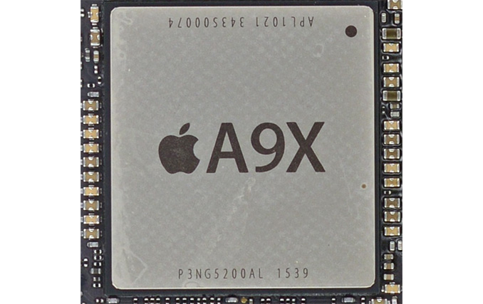
Over the Thanksgiving break the intrepid crew over at Chipworks sent over their initial teardown information for Apple’s A9X SoC. The heart of the recently launched iPad Pro, the A9X is the latest iteration in Apple’s line of tablet-focused SoCs. We took an initial look at A9X last month, but at the time we only had limited information based on what our software tools could tell us. The other half of the picture (and in a literal sense, the entire picture) is looking at the physical layout of the chip, and now thanks to Chipworks we have that in hand and can confirm and reject some of our earlier theories.
A9X is the first dedicated ARM tablet SoC to be released on a leading-edge FinFET process, and it’s being paired with Apple’s first large-format tablet, which in some ways changes the rules of the game. Apple has to contend with the realities of manufacturing a larger SoC on a leading-edge process, and on the other hand a larger tablet that’s approaching the size of an Ultrabook opens up new doors as far as space and thermals are concerned. As a result while we could make some initial educated guesses, we’ve known that there would be a curveball in A9X’s design, and that’s something we couldn’t confirm until the release of Chipworks’ die shot. So without further ado:

A9X Die Shot w/AT Annotations (Die Shot Courtesy Chipworks)
| Apple SoC Comparison | ||||||
| A9X | A9 | A8X | A6X | |||
| CPU | 2x Twister | 2x Twister | 3x Typhoon | 2x Swift | ||
| CPU Clockspeed | 2.26GHz | 1.85GHz | 1.5GHz | 1.3GHz | ||
| GPU | PVR 12 Cluster Series7 | PVR GT7600 | Apple/PVR GXA6850 | PVR SGX554 MP4 | ||
| RAM | 4GB LPDDR4 | 2GB LPDDR4 | 2GB LPDDR3 | 1GB LPDDR2 | ||
| Memory Bus Width | 128-bit | 64-bit | 128-bit | 128-bit | ||
| Memory Bandwidth | 51.2GB/sec | 25.6GB/sec | 25.6GB/sec | 17.1GB/sec | ||
| L2 Cache | 3MB | 3MB | 2MB | 1MB | ||
| L3 Cache | None | 4MB | 4MB | N/A | ||
| Manufacturing Process | TSMC 16nm FinFET | TSMC 16nm & Samsung 14nm |
TSMC 20nm | Samsung 32nm | ||
Die Size: 147mm2, Manufactured By TSMC
First off, Chipworks’ analysis shows that the A9X is roughly 147mm2 in die size, and that it’s manufactured by TSMC on their 16nm FinFET process. We should note that Chipworks has only looked at the one sample, but unlike the iPhone 6s there’s no reason to expect that Apple is dual-sourcing a much lower volume tablet SoC.
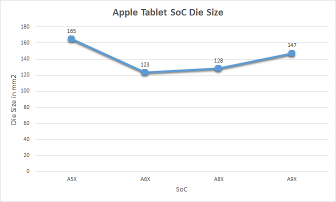
At 147mm2 the A9X is the second-largest of Apple’s X-series tablet SoCs. Only the A5X, the first such SoC, was larger. Fittingly, it was also built relative to Apple’s equally large A5 phone SoC. With only 3 previous tablet SoCs to use as a point of comparison I’m not sure there’s really a sweet spot we can say that Apple likes to stick to, but after two generations of SoCs in the 120mm2 to 130mm2 range, A9X is noticeably larger.
Some of that comes from the fact that A9 itself is a bit larger than normal – the TSMC version is 104.5mm2 – but Apple has also clearly added a fair bit to the SoC. The wildcard here is what yields look like for Apple, as that would tell us a lot about whether 147mm2 is simply a large part or if Apple has taken a greater amount of risk than usual here. As 16nm FinFET is TSMC’s first-generation FinFET process, and save possibly some FPGAs this is the largest 16nm chip we know to be in mass production there, it’s reasonable to assume that yields aren’t quite as good as with past Apple tablet SoCs. But whether they’re significantly worse – and if this had any impact on Apple’s decision to only ship A9X with the more expensive iPad Pro – is a matter that we’ll have to leave to speculation at this time.
Finally, it's also worth noting just how large A9X is compared to other high performance processors. Intel's latest-generation Skylake processors measure in at ~99mm2 for the 2 core GT2 configuration (Skylake-Y 2+2), and even the 4 core desktop GT2 configuration (Intel Skylake-K 4+2) is only 122mm2. So A9X is larger than either of these CPU cores, though admittedly as a whole SoC A9X contains a number of functional units either not present on Skylake or on Skylake's Platform Controller Hub (PCH). Still, this is the first time that we've seen an Apple launch a tablet SoC larger than an Intel 4 core desktop CPU.
GPU: PVR 12 cluster Series7
One thing we do know is that Apple has invested a lot of their die space into ramping up the graphics subsystem and the memory subsystem that feeds it. Based on our original benchmark results of the A9X and the premium on FinFET production at the moment, I expected that the curveball with A9X would be that Apple went with a more unusual 10 core PowerVR Series7 configuration, up from 6 cores in A9. Instead, based on Chipworks’ die shot, I have once again underestimated Apple’s willingness to quickly ramp up the number of GPU cores they use. Chipworks’ shot makes it clear that there are 12 GPU cores, twice the number found in the A9.
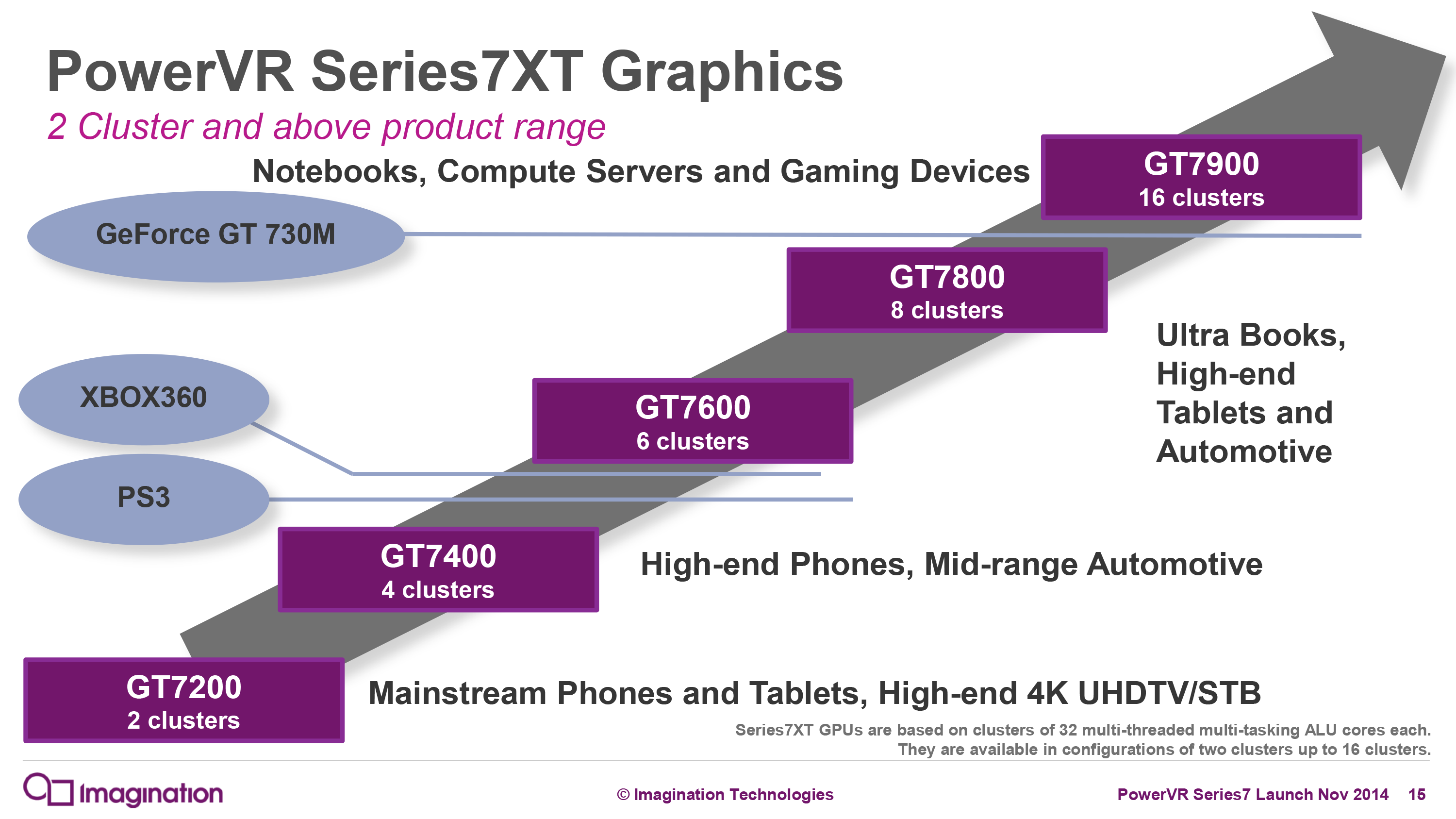
In Imagination’s PowerVR Series7 roadmap, the company doesn’t have an official name for a 12 core configuration, as this falls between the 8 core GT7800 and 16 core GT7900. So for the moment I’m simply calling it a “PowerVR 12 cluster Series7 design,” and with any luck Imagination will use a more fine-grained naming scheme for future generations of PowerVR graphics.
In any case, the use of a 12 core design is a bit surprising since it means that Apple was willing to take the die space hit to implement additional GPU cores, despite the impact this would have on chip yields and costs. If anything, with the larger thermal capacity and battery of the iPad Pro, I had expected Apple to use higher GPU clockspeeds (and eat the power cost) in order to save on chip costs. Instead what we’re seeing is a GPU that essentially offers twice the GPU power of A9’s GPU. We don’t know the clockspeed of the GPU – this being somewhat problematic to determine within the iOS sandbox – but based on our earlier performance results it’s likely that A9X’s GPU is only clocked slightly higher than A9’s. I say slightly higher because no GPU gets 100% performance scaling with additional cores, and with our GFXBench Manhattan scores being almost perfectly double that of A9’s, it stands to reason that Apple had to add a bit more to the GPU clockspeed to get there.
Meanwhile looking at the die shot a bit deeper, it’s interesting how spread out the GPU is. Apple needed to place 6 clusters and their associated shared logic on A9X, and they did so in a decidedly non-symmetrical manner. On that note, it’s worth pointing out that while Apple doesn’t talk about their chip design and licensing process, it’s highly likely that Apple has been doing their own layout/synthesis work for their PowerVR GPUs since at least the A4 and its PowerVR SGX 535, as opposed to using the hard macros from Imagination. This is why Apple is able to come up with GPU configurations that are supported by the PowerVR Rogue architecture, but aren’t official configurations offered by Imagination. A8X remains an especially memorable case since we didn’t initially know Series6XT could scale to 8 GPU cores until Apple went and did it, but otherwise what we see with any of these recent Apple SoCs is what should be a distinctly Apple GPU layout.
Moving on, the memory controller of the A9X is a 128-bit LPDDR4 configuration. With twice as many GPU cores, Apple needs twice as much memory bandwidth to maintain the same bandwidth-to-core ratio, so like the past X-series tablet SoCs, A9X implements a 128-bit bus. For Apple this means they now have a sizable 51.2GB/sec of memory bandwidth to play with. For a SoC this is a huge amount of bandwidth, but at the same time it’s quickly going to be consumed by those 12 GPU cores.
L3 Cache: None
Finally let’s talk about the most surprising aspect of the A9X, its L3 cache layout. When we published our initial A9X results we held off talking about the L3 cache as our tools pointed out some extremely unusual results that we wanted to wait on the Chipworks die shot to confirm. What we were seeing was that there wasn’t a section of roughly 50ns memory latency around the 4MB mark, which in A9 is the transfer size at which we hit its 4MB L3 victim cache.
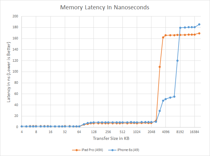
What Chipworks’ die shot now lets us confirm is that this wasn’t a fluke in our tools or the consequence of a change in how Apple’s L3 cache mechanism worked, but rather that there isn’t any L3 cache at all. After introducing the L3 cache with the A7 in 2013, Apple has eliminated it from the A9X entirely. The only cache to be found on A9X are the L1 and L2 caches for the CPU and GPU respectively, along with some even smaller amounts for cache for various other functional blocks.
The big question right now is why Apple would do this. Our traditional wisdom here is that the L3 cache was put in place to service both the CPU and GPU, but especially the GPU. Graphics rendering is a memory bandwidth-intensive operation, and as Apple has consistently been well ahead of many of the other ARM SoC designers in GPU performance, they have been running headlong into the performance limitations imposed by narrow mobile memory interfaces. An L3 cache, in turn, would alleviate some of that memory pressure and keep both CPU and GPU performance up.
One explanation may be that Apple deemed the L3 cache no longer necessary with the A9X’s 128-bit LPDDR4 memory bus; that 51.2GB/sec of bandwidth meant that they no longer needed the cache to avoid GPU stalls. However while the use of LPDDR4 may be a factor, Apple’s ratio of bandwidth-to-GPU cores of roughly 4.26GB/sec-to-1 core is identical to A9’s, which does have an L3 cache. With A9X being a larger A9 in so many ways, this alone isn’t the whole story.
What’s especially curious is that the L3 cache on the A9 wasn’t costing Apple much in the way of space. Chipworks puts the size of A9’s 4MB L3 cache block at a puny ~4.5 mm2, which is just 3% the size of A9X. So although there is a cost to adding L3 cache, unless there are issues we can’t see even with a die shot (e.g. routing), Apple didn’t save much by getting rid of the L3 cache.
Our own Andrei Frumusanu suspects that it may be a power matter, and that Apple was using the L3 cache to save on power-expensive memory operations on the A9. With A9X however, it’s a tablet SoC that doesn’t face the same power restrictions, and as a result doesn’t need a power-saving cache. This would be coupled with the fact that with double the GPU cores, there would be a lot more pressure on just a 4MB cache versus the pressure created by A9, which in turn may drive the need for a larger cache and ultimately an even larger die size.
As it stands there’s no one obvious reason, and it’s likely that all 3 factors – die size, LPDDR4, and power needs – all played a part here, with only those within the halls of One Infinite Loop knowing for sure. However I will add that since Apple has removed the L3 cache, the GPU L2 cache must be sizable. Imagination’s tile based deferred rendering technology needs an on-chip cache to hold tiles in to work on, and while they don’t need an entire frame’s worth of cache (which on iPad Pro would be over 21MB), they do need enough cache to hold a single tile. It’s much harder to estimate GPU L2 cache size from a die shot (especially with Apple’s asymmetrical design), but I wouldn’t be surprised of A9X’s GPU L2 cache is greater than A9’s or A8X’s.
In any case, the fact that A9X lacks an L3 cache doesn’t change the chart-topping performance we’ve been seeing from iPad Pro, but it means that Apple has once more found a way to throw us a new curveball. And closing on that note, we’ll be back in December with our full review of the iPad Pro and a deeper look at A9X’s performance, so be sure to stay tuned for that.
Source: Capped A9X Photo Courtesy iFixit


121 Comments
View All Comments
vFunct - Monday, November 30, 2015 - link
They have such a huge headroom if they ever want to increase their power budget from 5-10Watts and build a laptop (45 Watt) or even desktop/server (180 Watt) chip. Just upping the clock frequency by 50% and they'll already be faster than any Intel chip available.Combine this with high-bandwidth memory using through-chip Vias, or just adding tons of cache & cores, and there are amazing possibilities here. Apple really could compete hard against Intel in their core market.
nathanddrews - Monday, November 30, 2015 - link
I don't disagree, but I'll believe it when I see it.tipoo - Monday, November 30, 2015 - link
Firstly we don't know if it would scale that well, as a low power optimized architecture it may not be able to clock much higher than it is without lengthening the pipeline, and thus lowering IPC.And for your other statement, I recommend reading every page of this
http://www.pcworld.com/article/3006268/tablets/tes...
Mondozai - Monday, November 30, 2015 - link
The guy is using Tabletmark as a supposed cure to Geekbench. The problem is that a core i5 is scoring LESS than a weak-sauce core-M in photo/video editing work. Anyone who believes that deserves to be laughed at.Do you think that article has any validity at all? I'm fine with A9X skepticism vis-a-vis Intel but if you're going to do a hatchet job, at least do it correctly.
MrSpadge - Monday, November 30, 2015 - link
Didn't read your link, but the rest of your post hit's the nail on its head. And to push even further: if Apple somehow designed the A9(X) as a low power architecture which could still take 50% higher clock speeds, they would have designed it badly - because by designing for fixed low frequencies you can gain a lot of power efficiency. That's why CPUs like Dothan or Brazos don't clock all that high, no matter the voltage & power you give them.kaspar737 - Monday, November 30, 2015 - link
If you run a real benchmark like Linpack the results aren't even funny. The A9X does like 1/10th of a 5W Broadwell.melgross - Monday, November 30, 2015 - link
Show us some numbers then. Besides its not being used much anymore, as it isn't useful these days.kaspar737 - Monday, November 30, 2015 - link
http://www.techpowerup.com/forums/threads/processo...Couldn't find the 5W Broadwell results I once found, but here the 3317u (17W Ivy Bridge) is doing about 28 GFLOPS, even if you take off half the score because of multithreading and slightly higher clock, it still leaves you with 14 GFLOPS.
http://www.notebookcheck.net/Apple-A9-Smartphone-S...
The Apple A9 gets about 1.2 GFLOPS.
http://www.notebookcheck.net/Apple-A8X-iPad-SoC.12...
A8X gets 2.5 GFLOPS.
I couldn't find the A9X results yet but I believe they will be somewhere around 2GFLOPS.
jasonelmore - Monday, November 30, 2015 - link
this, apple is designing their soc to look good on geekbench, and other popular benchmarks with victim cache and optimized layout. They are gaming the results to make their chips look as powerful as Intel's Core Architecture. I dont blame them, everyone is doing it nowadays.But....When you throw pure math at it, the big boys separate from the small boys.
xype - Monday, November 30, 2015 - link
Uhm, so the benchmarks are what inform CPU design decisions, not actual, real world use cases in mobile devices? Because, to me, servers/laptops and mobile devices have _hugely_ different use cases; servers/desktops need to perform at a high load continuously, while mobile devices usually need bursts of (decent) performance and mainly good GPU capabilities.An iOS device’s main compute use case is drawing the UI, no? It stands to reason Apple would optimise for that and games. I’m sure they could also design a decent desktop CPU, but that wouldn’t be used in their mobile devices and, let’s face it, couldn’t easily beat Intel’s CPU designs (since Intel is not a bunch of amateurs).